
Vortex pinning
Type-II superconductors form vortices in an external magnetic field. Movement of these flux lines under influence of a current density j above a threshold jc (the critical current density) leads to a finite resistance. For technical application of such Superconductors, the vortices must be pinned, their mobility has to be decreased by implantation of defects (pinning sites) into the underlying crystal lattice.
The critical current density can be increased by immobilisation of vortices in the specimen by means of small regions with supressed superconductivity that exert attractive forces on a vortex and act as a pinning center. To be able to form a usable pinning center, the size of the weak spots should be in the order of the coherence length [1,2] or the magnetic penetration depth [3] of the material, which is in the order of some nm (approx. 10nm in Nb) at low temperatures. Larger pinning centers lead to formation of multiquanta vortices at the pinning centers and lower the efficiency of the pinning effects [2].
Furthermore, to be able to measure matching effects, a periodic order of these pinning sites is required, which, due to the very small scale, can hardly be produced by conventional lithgraphic techniques. To arrive at such arrays of nanoscaled artificial pinning centers, a patterning technique based on self-organization of Au-salt-loaded spherical micelles made of diblock-copolymers that form a triangular lattice of medium-range order over 4-8 lattice constants is applied. By plasma treatment, the polymer carriers are completely removed, while the metal salt is reduced to metallic nanoparticles, which still exhibit the original triangular order. Such particles deposited onto suitable substrates can be used as an etching mask to provide a corresponding triangular array of Si nanopillars or holes. The resulting structures are much smaller than those produced by conventional optical lithography techniques or by focused electron or ion beams.
 | 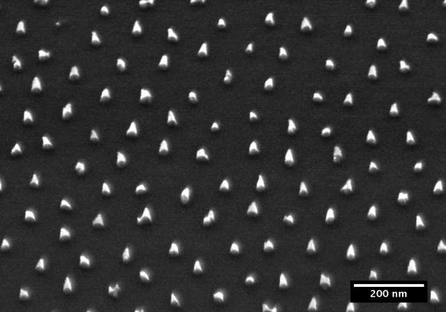 | 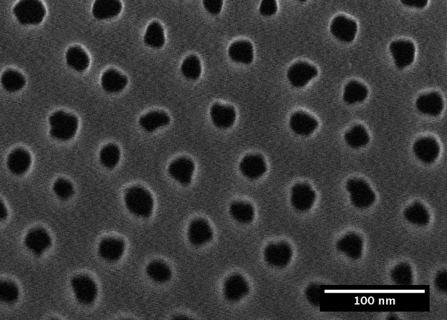 |
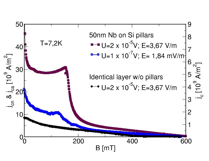
By growing a thin film of Niobium (or another superconducting material) on top of such a structured substrate, one ends up with a superconducting layer which contains a regular array of holes. In case of nanopillars, each of these holes is filled with one silicon pillar, nevertheless they act as effective pinning centers immobilizing magnetic flux lines in the superconducting material. To the best of my knowledge, these are the smallest ordered holes prepared into a superconducting thin film.
[1] G. S. Mkrtchyan and V. V. Shmidt, Sov. Phys. JETP 34:195 (1972)
[2] A. I. Buzdin, Phys. Rev. B 47(17):11416 (1993)
[3] N. Takezawa and K. Fukushima, Physica C 22:194 (1994)